
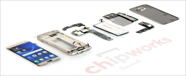
After the Galaxy S7 got the celebratory teardown treatment, its now its dual-edged bigger brother’s turn to lay on the disassembly table.
Canadian chip detectives Chipworks have gotten their meddling hands on the Galaxy S7 edge and are digging into its components as we speak.
Unlike other teardown websites which disassemble gadgets to rate their repairability, the guys at Chipworks are obsessed with figuring out every last chip and component’s origin, which makes their output all the more interesting, but also time-consuming. Therefore, their work happens in stages.
So far, so good, Chipworks has managed to take some brilliant shots of the GS7 edge’s internals and has come up with interesting observations on the smartphone’s camera setup and other components involved.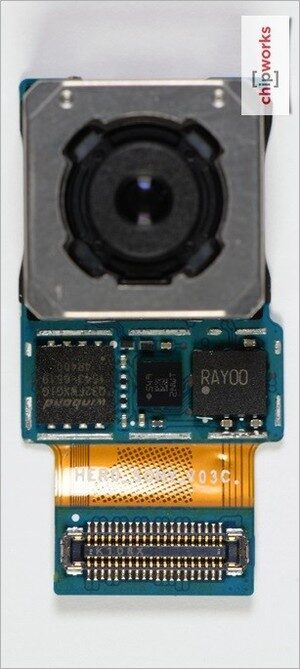
Galaxy S7 12 MP Rear-Facing Camera with Dual Pixel Autofocus (AF)
Just as Apple had, in 2013, reversed the pixel shrink trend of the time by transitioning from a 1.4 µm to 1.5 µm pixel pitch (iPhone 5 and 5s respectively), Samsung has similarly increased the pixel pitch of the Galaxy S7’s rear-facing camera. While the S6’s 16 MP camera featured 1.12 µm pitch pixels, the S7’s rear-facing camera now uses 1.4 µm generation pixels.
Apple has since settled in on a 12 MP resolution (currently with a 1.22 µm pixel pitch) for the iPhone 6s/6s Plus cameras. Samsung now meets Apple head-to-head at the 12 MP resolution with its larger pixels. We’ll have to wait and see who wins the image quality battle; as of now, DxOMark Mobile does not have a score for the S7/S7 Edge. Currently tied for 1st place are Sony’s Xperia Z5 camera, which features a 23 MP sensor with 1.12 µm pitch pixels, and the 16 MP Samsung Galaxy S6 Edge Plus camera.
So what is new with the S7’s camera system? Dual pixel phase detection autofocus (PDAF) technology! We first saw this concept in use in 2013 in a much different imaging application: the Canon EOS 70D DSLR. Canon committed 80% of the 70D’s active pixel array to dual pixel CMOS AF functionality. A similar concept has now been adapted to the world of small-pixel mobile camera chips, where 100% of the 12 MP active pixel array is committed to both sensing and providing data to the AF system.
What is impressive about the new dual pixel feature is the chip design team’s ability to roll out this technology in a 1.4 µm pixel generation (Canon’s DSLR system used 4.1 µm generation pixels). The results are stunning – the S7’s photos are of high quality, especially when viewed on its Quad HD display. We haven’t seen a claim for the S7’s AF system speed yet. As a reference point, Sony has reported a 0.03-second focus speed for its hybrid (contrast and phase detection) AF system in the Xperia Z5.
We’ll be doing more thorough analysis of the dual pixel technology over the coming days and weeks, but our initial review of the 12 MP camera module shows a camera module size of 12.1 mm x 12.1 mm x 5.4 mm thick. We’ve been reading the web articles indicating a Sony IMX260 design win for the 12 MP socket and we’re eagerly awaiting results from our lab to confirm. Based on the “SONY” logo on the module’s flex cable, we believe the speculation to be true.
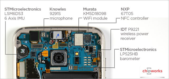
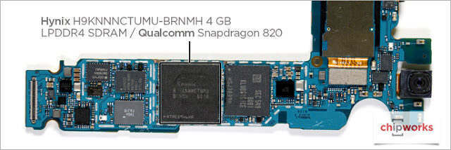
There are other interesting observations, too. Apparently, Samsung adopted their own S6SMC41X touch screen controller (TSC) in their own phone for the first time. Chipworks first saw it in Chinese brand Doov’s L5Pro phone a few weeks ago. Curiously, though, the LPDDR4 RAM memory is supplied by Hynix, rather than Samsung’s own and very successful LSI division. It’s probably Samsung Mobile differentiating suppliers, rather than relying on Hynix as the sole provider.
Chipworks also confirmed the Qualcomm Snapdragon 820 chipset carries the model number ‘MSM8996’, and noticed “a large increase in the interconnecting solder bumps”between the chipset and RAM memory (assembled in a package-on-package format) which could be due to the higher memory bandwidth and/or heat dissipation concerns.
The nimble Canadians will be updating their publication as they get other sections of the Galaxy s7 edge examined, so check out the source link below for the full story and images. This is excellent work on Chipworks’ part and we’ll be watching its ongoing development with interest, along with many of you!
Via ChipWorks

- Top 10 Best Samsung Galaxy S23 Camera Apps - September 5, 2023
- Download 4D Parallax Wallpapers App Galaxy 24 Ultra - September 5, 2023
- How to Delete or Deactivate Instagram Account Permanently? - September 5, 2023